Russia Breaks Sanctions Wall: New Progress STP-350 Chip Machine Could Reshape Military Technology Power Balance
Russia’s domestically developed Progress STP-350 photolithography machine is emerging as more than a semiconductor breakthrough, potentially strengthening Moscow’s military-industrial resilience while exposing limitations in technology denial strategies designed to constrain strategic adversaries.

(DEFENCE SECURITY ASIA) — The appearance of Russia’s first domestically commercialized photolithography system is rapidly emerging as a strategic development extending far beyond semiconductor manufacturing because it directly intersects with sanctions warfare, military resilience, and the future balance of technological power.
At a time when export controls were designed to constrain Moscow’s access to advanced semiconductor equipment, the launch of the Progress STP-350 instead signals a broader geopolitical reality in which technological denial strategies increasingly face adaptation, localization, and industrial countermeasures.
Russian industrial officials and technical analysts have effectively framed the Progress STP-350 as a sovereignty project rather than a commercial electronics initiative, emphasizing that battlefield resilience and strategic continuity increasingly outweigh raw computational performance in contemporary military planning.
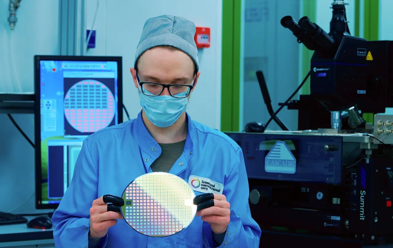
Developed by Moscow-based Zelenograd Nanotechnology Center, the Progress STP-350 entered open sale at the end of 2025 and represents Russia’s first domestically developed photolithography machine intended for serial industrial deployment.
The first machine was reportedly delivered to a buyer associated with the Element Group, establishing the transition from prototype status into operational commercial availability within Russia’s strategic microelectronics ecosystem.
The system enters service at a moment when semiconductor supply chains have become central instruments of geopolitical coercion, making lithography capabilities increasingly comparable to strategic energy infrastructure or critical defense industrial assets.
Rather than pursuing direct competition against leading-edge commercial semiconductor manufacturers, Russian planners appear to have adopted a more focused industrial doctrine centered on battlefield survivability and sanctions endurance.
This approach suggests Russia is prioritizing strategic utility over technological prestige by targeting semiconductor categories most directly linked to military reliability requirements.
Western observers have frequently highlighted Russia’s lag behind frontier semiconductor technologies, yet the Progress STP-350 demonstrates that military requirements often diverge fundamentally from consumer electronics priorities.
The resulting development therefore carries implications extending beyond Russia because sanctioned states worldwide increasingly observe whether technological sovereignty can be rebuilt under external pressure.
The emergence of the Progress STP-350 also reinforces a broader strategic lesson that semiconductor competition increasingly concerns control over industrial production ecosystems rather than merely achieving leadership in transistor miniaturization metrics.
For defense planners and sanctions architects alike, Russia’s latest move introduces a difficult strategic question regarding whether technological containment remains sustainable when mature-node capabilities can still preserve warfighting capacity and critical infrastructure continuity.
READ: Russia’s New Su-57D Two-Seat Stealth Fighter Sparks Global Alarm: Drone-Command “Felon” Could Reshape India-China Airpower Balance
Mature Node Technology Built for Battlefield Survivability
The Progress STP-350 operates using a 350 nanometer process node based on mature i-line stepper lithography technology optimized around reliability rather than computational density.
Although modern smartphones and artificial intelligence accelerators increasingly rely on five to seven nanometer architectures, larger transistor geometries frequently provide significant operational advantages under severe environmental stress conditions.
Larger and thicker transistor structures generated at 350 nanometers exhibit greater resistance to radiation exposure, electromagnetic interference, and electrical instability than ultra-miniaturized semiconductor designs.
This design philosophy reflects longstanding aerospace and military engineering doctrine where predictable survivability frequently supersedes performance benchmarks measured under controlled laboratory environments.
Russian analysts emphasize that battlefield electronics experience operating conditions fundamentally different from civilian consumer products because combat systems face vibration, heat fluctuations, and electromagnetic disruption.
The Progress STP-350 reportedly supports semiconductor structures capable of handling voltages reaching approximately 100 volts, creating advantages in power electronics and military control systems.
The architecture also permits deployment across environments involving substantial temperature variations that can degrade smaller semiconductor geometries.
These characteristics reportedly make the chips suitable for combat platforms including missile guidance systems, radar modules, aircraft control units, and power distribution systems.
For strategic military applications, component survivability often determines operational effectiveness more than raw processing speed or transistor density.
Triple-Redundant Design Strengthens Strategic Reliability
One of the most significant military implications surrounding the Progress STP-350 involves its compatibility with triple-redundant electronic architectures used in mission-critical systems.
Triple redundancy involves operating three identical processing pathways simultaneously so individual component failures do not produce catastrophic system breakdowns.
Such architectures are particularly relevant for strategic systems where radiation exposure or electromagnetic pulse effects could disrupt individual semiconductor components.
Russian analysts argue that larger transistor structures demonstrate greater resilience against cosmic radiation interference capable of inducing electronic faults in advanced miniature geometries.
Modern semiconductor miniaturization increasingly creates vulnerability because smaller electrical thresholds become more sensitive to disruption from radiation and electromagnetic anomalies.
Military platforms operating in high-altitude environments or nuclear scenarios frequently prioritize hardened electronics capable of preserving system integrity during extreme events.
The Progress STP-350 therefore supports requirements extending beyond ordinary battlefield operations toward strategic deterrence and critical infrastructure resilience.
Applications reportedly include missile control systems, aerospace hardware, and combat command networks where reliability failures remain operationally unacceptable.
Such requirements illustrate why mature semiconductor nodes continue retaining military relevance despite appearing technologically outdated from commercial perspectives.
Solid-State Laser Design Marks Technical Evolution
The Progress STP-350 replaces older mercury lamp technologies with a modern solid-state laser operating around 365 nanometers.
This transition introduces improvements in energy efficiency, optical coherence, brightness stability, and operational longevity compared with legacy illumination systems.
Technical documentation indicates operational lifespan reaching approximately 10,000 hours, substantially reducing maintenance requirements and improving industrial throughput sustainability.
The machine reportedly processes up to 63 silicon wafers hourly using 150-millimeter substrates and approximately 43 wafers for larger 200-millimeter wafers.
It accommodates six-inch and eight-inch silicon wafer formats frequently used within industrial and military semiconductor production environments.
The system employs five-to-one optical reduction capabilities alongside alignment precision reportedly ranging between approximately 65 and 90 nanometers.
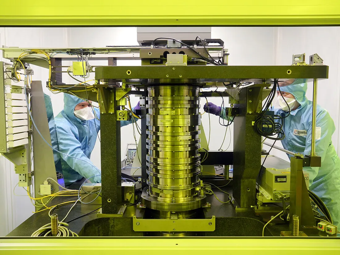
Physically, the optical-mechanical architecture weighs roughly 3.5 tons and incorporates substantial industrial infrastructure requirements.
These characteristics collectively indicate that Progress STP-350 represents an operational manufacturing system rather than an experimental laboratory demonstrator.
For Russia’s semiconductor sector, possessing domestic lithography machinery introduces strategic independence extending beyond individual component production.
Belarus Partnership Reveals Strategic Technology Axis
Development of the Progress STP-350 reportedly began during 2021 through Ministry of Industry and Trade initiatives focused on import substitution.
The project received contracts valued between approximately 7.5 billion and 7.9 billion rubles, representing roughly USD95 million to USD100 million or RM361 million to RM380 million using prevailing conversion assumptions.
A key enabling factor involved cooperation with Belarusian company Planar, which retained significant Soviet-era semiconductor engineering expertise.
Planar reportedly contributed baseline machine architecture derived from EM-5884 stepper technologies while supporting localization and adaptation efforts.
Russian sources claim this partnership reduced Moscow’s technological gap from approximately forty to fifty years behind Western lithography leaders toward an estimated thirty-year disparity.
The project simultaneously strengthened industrial integration within the Russia-Belarus technological framework.
This cooperation highlights how strategic alliances increasingly serve as pathways for technological resilience among geopolitically constrained states.
Rather than complete domestic isolation, the initiative reflects selective industrial partnerships structured around sovereignty objectives.
The Russia-Belarus technology relationship therefore increasingly resembles a strategic industrial ecosystem rather than ordinary commercial collaboration.
READ: Russia Deploys Pacific Fleet to Shield Sanctioned ‘Shadow Fleet’ Through Tsushima Strait, Triggering Indo-Pacific Maritime Security Alarm
Sanctions Resilience and Future Semiconductor Competition
The base Progress STP-350 reportedly enters the market at approximately 392 million rubles equivalent to roughly USD4.5 million or RM17.1 million.
Configurations including extended service support and five-year warranties reportedly reach approximately 561 million rubles or approximately USD6.4 million and RM24.3 million.
Russian specialists reportedly characterize this pricing structure as competitive because comparable foreign systems frequently cost two to three times more.
The machine’s broader significance nevertheless extends beyond pricing because control over lithography equipment effectively determines long-term industrial autonomy.
Before localization efforts, Russia relied substantially upon imported equipment for even mature semiconductor manufacturing processes.
By securing domestic production pathways for lithography machinery itself, Russia gains control over foundational industrial infrastructure supporting future military electronics manufacturing.
Moscow is reportedly already pursuing a follow-on 130 nanometer platform expected to represent the next critical benchmark for technological progression.
Western critics continue arguing that 350 nanometer technology remains fundamentally symbolic because frontier semiconductor competition increasingly revolves around vastly smaller architectures.
Yet the strategic issue may ultimately concern whether technological denial can permanently constrain military-industrial resilience because Russia appears increasingly focused on ensuring that critical weapons systems continue functioning even under complete isolation from Western supply chains.